

Multi-reticle packages – optical devices with multiple reticle patterns that are user-switchable as needed – are becoming increasingly common as hyper-scale computing and other applications such as artificial intelligence (AI) adopt 2.5D to 3.5D device packaging. The advanced packaging industry, in turn, is implementing larger, panel-level packaging (PLP) to improve yield and increase throughput for these devices. TSMC, Intel, and outsourced semiconductor assembly and test (OSAT) companies are rapidly adopting PLP to meet the growing demand for multi-reticle packages.
A critical process in overall PLP packaging is bumping to connect the die or chiplets together to create the final package. A key ingredient in getting the bumps to attach to the die and then reflow properly is the flux material. The responsibility of the flux material is to remove impurities and oxides from the surface of the solder balls during the reflow process. This allows the solder balls to melt uniformly and provide a clean surface1. However, once reflow is completed, the flux becomes a contaminant that could create shorts in the package and thus needs to be removed before the next process step to prevent potential electrochemical migration and result in a defect-free underfill process.
Panel-Level Packaging Cleaning Challenges
In PLP cleaning, the flux presents additional challenges. The panels are larger substrates compared to those used in the past. PLP uses panels that are either 515mm x 510mm or 600mm x 600mm, which is a significant jump in size compared to the 300mm substrates currently used in packaging.
Cleaning larger panel sizes with more die increases cleaning complexity compared to wafer-level packaging (WLP). PLP’s shift toward smaller bump pitches creates smaller spaces between die, increasing the surface tension and limiting liquid penetration, which hinders the cleaning of bump pitches under 20 micron (µm). Issues like corrosion, delamination, and device failure that can result from incomplete cleaning could prove very costly in larger packages.
PLP’s larger substrate sizes and smaller features create unique requirements for which new, sophisticated cleaning process technology is needed. The new technology must take into consideration how cleaning under atmospheric pressure can leave residue and moisture due to the higher surface tension and smaller spaces. Conventional technology can lead to poor wetting and inhibit the liquid flow into smaller, more narrow spaces. Traditional technology is ineffective for next-generation packages with smaller features that require higher levels of flux for successful process results.
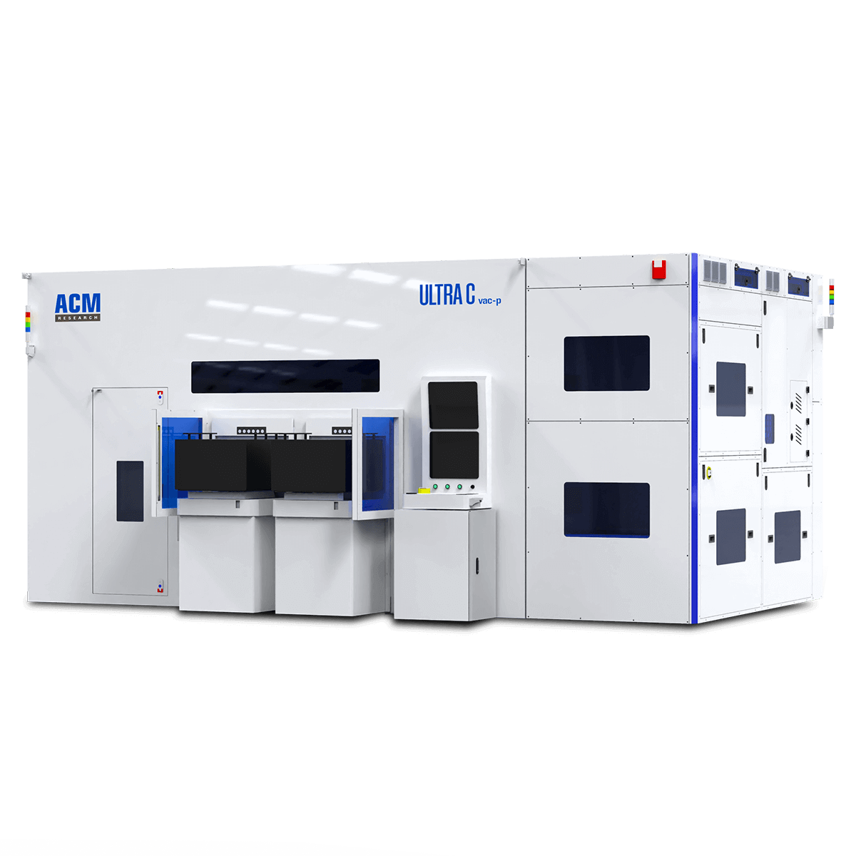
Ultra C vac-p Tool: Flux Cleaning Capabilities
At ACM Research, we have leveraged our expertise in packaging clean technology to develop the Ultra C vac-p tool, specifically designed for PLP flux cleaning. The Ultra C vac-p features vacuum-base cleaning, which results in more efficient residue removal. The tool can support a saponification agent for cleaning packages with high flux to ensure complete cleaning. Our tool’s high-pressure spray and direct chemical application targets the increasingly intricate geometries emerging in advanced PLP designs.
Our tool is also fully customizable and configurable for various panel sizes and die quantities, addressing diverse panel materials and flux types. The design and process chemistries of our tool also ensure uniform cleaning across the larger panels.
The Ultra C vac-p offers highly reliable and efficient cleaning due to its ability to work with multiple panel sizes and to clean different flux types. Combining environmentally friendly processes and cleaning agents with vacuum technology ensures a flux-free surface with low defects.
ACM Research’s Ultra C vac-p is designed to meet the emerging needs of panel-level processing for hyper-scale computing and AI applications by providing a superior solution for flux-cleaning panels, resulting in packages with lower defects and higher yields.
References: