

Part one of this blog series on optimizing wafer-level through-silicon vias (TSV) for heterogeneous integration of multiple components and 2.5D/3D packaging provided an overview of the TSV formation process and elucidated post via cleaning solution. The SAPS™ megasonic technology developed by ACM Research enables chipmakers to remove residue following TSV formation much more effectively and completely than other megasonic or jet spray processes. In part two, we turn to electroplating.
Electroplating is an essential process in TSV fabrication. Once the vias have been thoroughly cleaned, and conformal linear and seed layer have been deposited, they are subsequently filled with electroplating of metal, typically copper. Void-free electroplating of Cu in high-aspect-ratio features is vital to deliver low resistivity and high reliability for transistor performance. However, void-free fill and uniform deposition at high plating rate are challenging to achieve with conventional deposition tools. Mass transport limitation reduces the deposition rate, and results in voids in the vias and uneven Cu surface. ACM Research’s Ultra ECP system has expertise in integrating the optimal Cu plating into the TSV formation process.
Ultra ECP for WLP
ACM Research’s Ultra ECP platform includes two systems that target wafer-level packaging: Ultra ECP ap and Ultra ECP 3d (see Figure 1). Ultra ECP ap system supports Cu via filling and Cu pillar bumping for Cu, it delivers high-speed plating technology for uniform deposition in vias without sacrificing plating rate. Ultra ECP 3d is integrated with ACM Research’s exclusive Multi-Anode Partial Plating function, which allows the deposition of Cu metal layer on via structures of 3D TSVs and 2.5D interposers, and is compatible with aspect ratios of 10:1 and beyond.
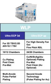
Figure 1. ACM Research’s Ultra ECP portfolio includes the Ultra ECP 3d and Ultra ECP ap models for WLP. ACM Research’s second anode and chamber paddle technologies deliver distinct advantages over other plating systems on the market.
Second-anode design
Traditionally, electroplating systems utilize a single anode, limiting the deposition rate and uniformity across the wafer surface. The addition of a second anode in the Ultra ECP platform enables precise control over current distribution during the electroplating process, minimizing variations in plating thickness and improving overall uniformity. This innovation results in more consistent deposition rates and better quality of plated layers, leading to higher yields and improved device performance as well as better process times and throughputs.
Additional benefits
The Ultra ECP ap also features a dual-anode design for better uniformity across the wafer. With two anodes, Ultra ECP ap enables independent control over deposition rates and characteristics, providing finer granularity in adjusting plating parameters. The dual-anode configuration also offers compatibility with a wide range of substrates, materials and metals, including copper, nickel, and tin-silver (SnAg), an alloy that is growing in popularity due to its high stability.
Once your well-formed TSVs have been thoroughly cleaned and uniformly plated to ensure high-quality interconnects within 2.5D/3D structures, the next step is polishing to remove the excess metal and barrier layers in the field regions. Part three of this series will examine ACM Research’s stress-free polishing (SFP) technology.