Panel Level Packaging—Ultra ECP ap-p

Panel-Level Copper Deposition for Fan-Out Panel-Level Packaging
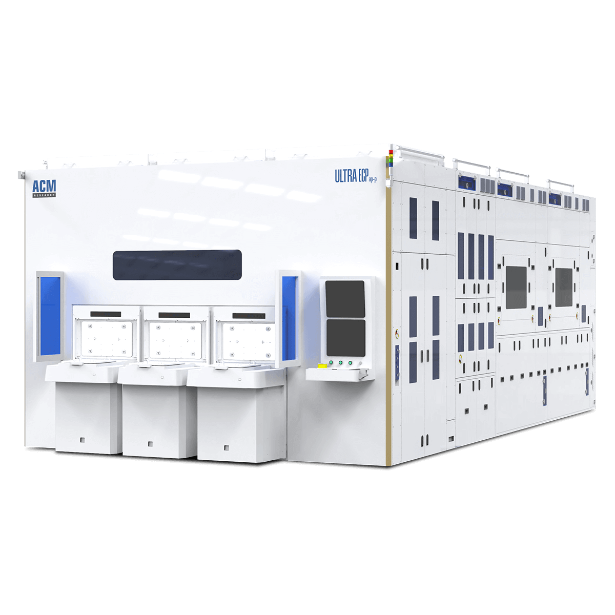
The Ultra ECP ap-p draws upon ACM’s deep-rooted expertise in wafer plating and copper processes for advanced packaging and is the first commercial high-volume panel-level packaging copper deposition system ready for the large-panel market. The Ultra ECP ap-p supports advanced fan-out panel-level packaging (FOPLP) with submicron features on large panels, which are applicable to artificial intelligence (AI) applications using large chiplet graphic processing units (GPUs) and high-density high-bandwidth memory (HBM).
The Ultra ECP ap-p can be used for plating steps in variety of processes including pillar, bump, and RDL. The panel plating equipment can also be utilized for micron- and sub-micron high-density panel level packaging.
Major Benefits of ECP for Panel Level Packaging
- Horizontal chamber configuration provides high plating efficiency and excellent uniformity, and it eliminates the potential for cross-contamination.
- Provides individual chamber maintenance that increases equipment uptime.
- Uniform electric field distribution within the panel to achieve good film thickness uniformity within panel and panel-to-panel.
Equipment Specifications
- Capable of running 510 x 515 mm and 600 x 600 mm panels
- Configuration of up to 3 load ports
- Equipped with 2 pre-wet chambers and 2 clean chambers
- Equipped with alignment and charge-coupled device (CCD) edge inspection, as well as a flip unit
- Can be equipped with up to 16 plating chambers for copper, nickel, tin-silver, gold, etc.
- Warpage: ≤10 mm
Process Index of Ultra ECP ap-p
- Within-wafer uniformity: <5% (max-min/2Ave.)
- Within-die uniformity: <5% (max-min/2Ave.)
- Repeatability: <3%

Contact Us
Looking for spare parts and customer support for your ACM Research Systems?
