The 3D packaging sector has been growing rapidly, driven by the expansion of chiplet packaging across the ecosystem. Chip and package sizes have also grown rapidly as 2 x 800mm2 chips are being placed in a single package along with high-bandwidth memory (HBM). Demand for these large chiplets has generated supply constraints due to how the chips are packaged – fan-out wafer level packaging (FOWLP) is currently the primary methodology.
To help resolve packaging supply chain constraints, the advanced and chiplet packaging industry is moving from round substrates to square panels. Wafer manufacturers and outsourced assembly and test (OSAT) suppliers have both proposed using square glass panel substrates to package large-area chiplets. This will significantly increase the number of chips that can be processed on a single panel.
Transitioning to panel-level packaging (PLP) has some additional advantages over WLP. For example, PLP enables the industry to significantly increase the substrate area for building chiplets and lowering packaging costs. The larger area allows more chips to be assembled in parallel, increasing capacity and thus helping to ease current supply constraints.
FOPLP will ease integrating various die technologies (e.g., logic, memory, and RF) into a single package, thus supporting more complex system designs. By utilizing fan-out techniques, designs can achieve the thinner profile and smaller footprint essential for modern consumer electronics. PLP integration can:
- Improve chiplet performance for the massive amounts of data being processed by artificial intelligence (AI), as well as in other compute-heavy applications;
- Assist with the implementation of HBM to help reduce compute times and power usage; and
- Allow for more efficient package device design, as opposed to the more typical board-level packaging approach.
Ultra ECP ap-p Capabilities
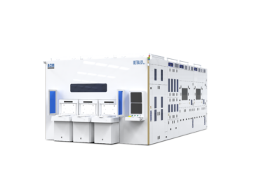
At ACM Research, we have leveraged our deep-rooted expertise in wafer electrochemical plating (ECP) and copper processes for advanced packaging to develop the first commercial high-volume PLP copper deposition system targeting the large-panel market.
Our Ultra ECP ap-p tool will enable advanced FOPLP with submicron features on large panels, which are applicable for AI applications using large-chiplet graphics processing units (GPUs) and high-density HBM. The Ultra ECP ap-p can be used for plating steps in a variety of processes, including pillar, bump, and redistribution layer (RDL), as well as for fan-out and through-glass via (TGV) processes.
The system is designed to handle organic and glass substrates sized 510mm x 515mm and 600mm x 600mm, while effectively managing cover warpages up to 7mm. To achieve this, we’ve integrated innovative robot and chuck systems that give us a competitive advantage in this space. These advanced automation features enhance efficiency and quality control throughout the manufacturing process and adapt traditional wafer-processing steps for larger and heavier panels. Included are critical operations like panel flipping for correct orientation and face-down plating.
The tool has up to 16 plating chambers and can deposit copper, nickel, tin-silver, gold, and other plating materials. We developed the system with a unique chamber configuration that provides high plating efficiency with both excellent uniformity and no cross-contamination, which can be a problem for systems that handle the panels vertically. In addition, the multi-anode area distribution effectively controls the height of the edges and corners of the panel.
The newest addition to our family of Ultra ECP tools, the Ultra ECP ap-p offers the industry unique capabilities for PLP copper deposition. As FOPLP gains further momentum, we look forward to playing a significant role in enabling the technology’s advancement.

ACM Research’s Ultra ECP ap-p tool is a first-of-its-kind commercial, high-volume PLP copper-deposition system that provides cost-effective, high-yield FOPLP processing technology for the advanced and chiplet packaging market.


