Throughout this blog series, we’ve taken you on a journey through the various steps involved in developing and optimizing through-silicon vias (TSVs), which have become vital to packaging of many types of devices that require smaller-footprint, higher-density package stacks. Part 1 discussed TSV formation and the benefits of our SAPS™ megasonics for TSV cleaning; Part 2 explained electroplating and how our Ultra ECP system optimizes copper fill in the vias; and Part 3 examined the problem of TSV gaps and the solution that we’ve developed to mitigate this issue: our Ultra Pmax plasma-enhanced chemical vapor deposition (PECVD) solution. This last installment focuses on the final step: polishing. We will look at why the polishing step is so critical to TSV formation, how stress-free polishing is shaping the future of semiconductor manufacturing, and the market advantages brought by our Ultra Stress-Free Polishing solution.
The role of polishing in TSV formation
Chemical mechanical planarization (CMP) is essential for ensuring that the wafer surface is planar and free of defects, which is critical for subsequent manufacturing steps such as wafer bonding or further lithography. Achieving a perfectly flat surface allows for the reliable connection of vertical interconnects between different layers of the 3D IC. Any variation in the surface topography can lead to electrical shorts, misalignment, and overall device failure. Therefore, the polishing step is indispensable for producing high-performance, reliable semiconductor devices with TSVs.
One of the major issues manufacturers face is managing mechanical stress during the CMP process. Mechanical stress can cause a range of defects, including wafer warping, TSV delamination, dishing, and micro-cracking, all of which reduce yield and impact the reliability of the final product. These defects become even more problematic as via sizes shrink and TSV densities increase. This is where stress-free polishing becomes critical.
The science of stress-free polishing
Traditional CMP processes involve a combination of chemical reactions and mechanical force to remove excess material and smooth the wafer’s surface. However, this mechanical force can introduce stress into the wafer, particularly in thinner wafers or those with densely packed TSVs. Mechanical stress is especially dangerous because it can cause latent defects that may not be immediately detectable but could lead to long-term reliability issues.
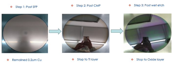
Stress-free polishing (SFP), as shown in Figure 1, seeks to minimize the mechanical forces exerted on the wafer during the CMP process. This is achieved by refining the polishing pad’s contact with the wafer, using advanced slurry formulations, and optimizing process conditions. By reducing the overall stress on the wafer, manufacturers can achieve better planarity and avoid defects like warpage and TSV delamination. The result is a higher-quality product with improved yield and performance.

Figure 1. Stress-free polishing provides a smooth wafer surface, with no mechanically induced TSV stresses or damage, facilitating CMP and wet etch steps.
Ultra SFP: Revolutionizing TSV polishing
We developed our Ultra Stress-Free Polishing (SFP) solution to meet the increasing demands of TSV manufacturing. This advanced technology offers several advantages over traditional CMP, making it particularly well-suited for TSV formation in high-performance and high-density semiconductor applications.
As the industry moves toward thinner wafers for improved performance and energy efficiency, Ultra SFP is specifically designed to handle these fragile substrates without introducing damage, unlike traditional CMP techniques. With its more refined polishing process, Ultra SFP greatly reduces the amount of mechanical force applied to the wafer, ensuring minimal stress. This is crucial in preventing common defects like TSV cracking, delamination, and wafer warpage. All of these defects affect planarity, which is key for ensuring that subsequent layers in the 3D IC stack align perfectly. Ultra SFP provides superior control over surface uniformity, leading to excellent planarization across the entire wafer.
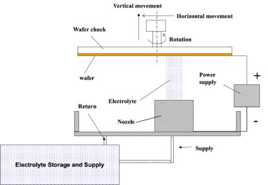
Another key advantage of Ultra SFP is its environmentally focused design (Figure 2). The tool has a built-in system for electrolyte recycling and reuse, enabling it to consume significantly fewer chemicals during processing. This enables semiconductor makers to improve their manufacturing sustainability for CMP and wet etch.

Figure 2. ACM Research’s Ultra SFP system features an environmentally friendly design that provides a real-time supply of electrolytes and enables recycling of used electrolytes regardless of Cu ion concentration.
By minimizing the potential for stress-related defects, Ultra SFP helps manufacturers improve yield rates. Fewer defective wafers mean lower production costs, making Ultra SFP an attractive solution for high-volume manufacturing environments and applications such as high-performance computing (HPC), artificial intelligence (AI), and automotive. Ultra SFP’s scalability makes it a flexible solution capable of addressing the increasing complexity of next-generation semiconductor devices.
Conclusion
The need for advanced TSV technology continues to escalate in parallel with semiconductor industry development. The polishing step in TSV formation is critical for ensuring the integrity and performance of these devices, and stress-free polishing is now more important than ever. ACM Research’s Ultra SFP solution offers a cutting-edge approach to overcoming the challenges of TSV manufacturing, providing the industry with a robust, scalable, and cost-effective tool to meet the demands of next-generation technologies.
By reducing mechanical stress and enhancing planarity, Ultra SFP ensures that manufacturers can produce higher-performance semiconductor devices while reducing the risk of costly defects. As TSV technology plays an ever-expanding role in enabling advanced packaging for AI, HPC, automotive systems, and other fast-evolving markets, innovations like ACM Research’s Ultra SFP will help pave the way for the future of semiconductor manufacturing.


